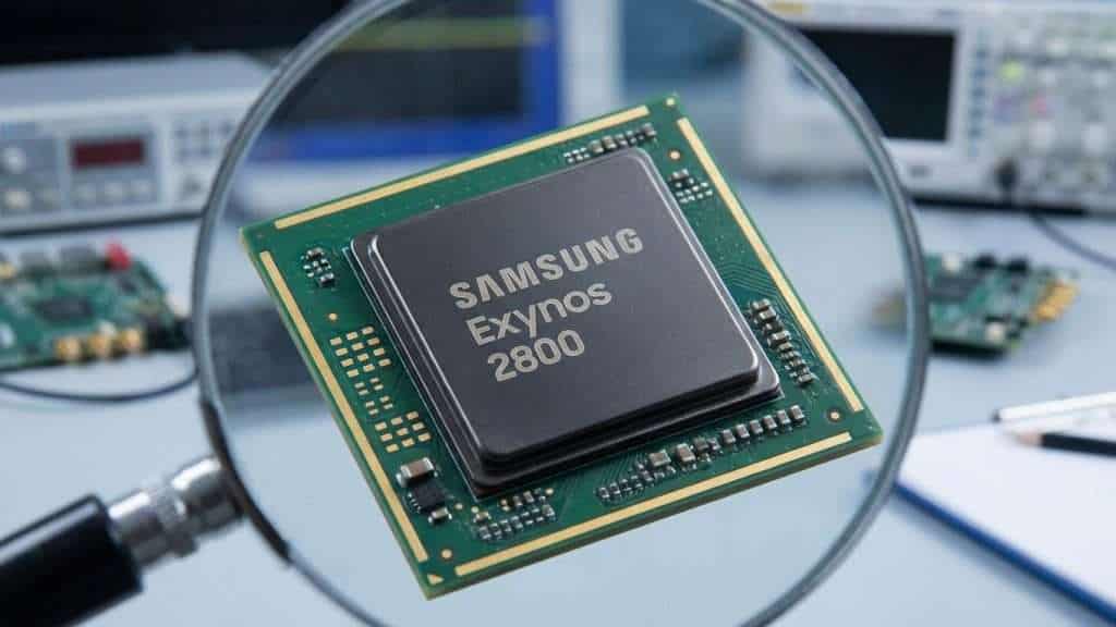
Samsung Shifts Focus to 2nm GAA Technology in Texas
Samsung is making a bold move in semiconductor manufacturing by accelerating its 2nm Gate-All-Around (GAA) technology production at its Taylor plant in Texas. Originally slated to focus on 4nm chip fabrication, the facility is now gearing up to mass produce 2nm wafers, signalling a significant strategic pivot that could position Samsung as a formidable competitor to TSMC in the U.S. market. This shift comes amid TSMC’s reluctance to deploy its most advanced nodes on American soil, opening a window of opportunity for Samsung to expand its presence.
Upgraded Production Capacity and Key Partnerships
The Taylor plant’s initial target was to produce 20,000 wafers per month, but recent reports indicate that Samsung has increased this goal to 50,000 monthly units. This ramp-up is supported by the installation of advanced EUV (extreme ultraviolet) lithography machinery, crucial for manufacturing sub-5nm chips with high yields. Samsung’s first 2nm GAA chipset, the Exynos 2600, has already entered mass production with an estimated 50% yield, which is expected to improve as the process matures.
Further bolstering Samsung’s ambitions, the company secured a $16.5 billion contract with Tesla to manufacture the AI6 chip, designed for next-generation autonomous driving applications. Additionally, Samsung is fulfilling 2nm GAA orders for two Chinese cryptocurrency hardware manufacturers, although production for these clients is likely to remain in South Korea rather than at the U.S. facility.
Context and Future Prospects
The Taylor plant’s transition from 4nm to 2nm GAA technology reflects Samsung’s determination to close the gap with TSMC, which currently leads in advanced node manufacturing. Industry insiders believe this move is part of a broader strategy to match TSMC’s scale, with expectations that the Texas facility could reach a monthly capacity of 100,000 wafers by 2027. Samsung has reportedly completed the basic design of its next-generation 2nm process, known as SF2P+, which is a third-generation 2nm GAA variant under development and may be implemented within the next two years.
This rapid progress highlights Samsung’s commitment to innovation and its efforts to establish a strong foothold in the competitive semiconductor landscape, particularly within the U.S. market where geopolitical factors influence manufacturing decisions.
What to Watch Next
As Samsung accelerates its 2nm GAA production and expands capacity at the Taylor plant, industry watchers will be keen to see how this affects the competitive dynamics with TSMC. The success of Samsung’s advanced node manufacturing in the U.S. could have significant implications for the semiconductor supply chain and the broader tech industry. Keeping an eye on yield improvements, production volumes, and new client partnerships will be essential in the coming months.
For more detailed insights, the original report from Munhwa provides an in-depth look at Samsung’s evolving strategy and production plans.