Samsung Advances Semiconductor Manufacturing with EUV Testing in Texas
Samsung is making significant strides towards establishing the United States as a hub for cutting-edge semiconductor production. The company is set to commence test operations of its extreme ultraviolet (EUV) lithography equipment at its Taylor plant in Texas starting this March. This move brings Samsung closer to its ambitious goal of mass producing next-generation 2nm gate-all-around (GAA) wafers on American soil, marking a major milestone in semiconductor manufacturing.
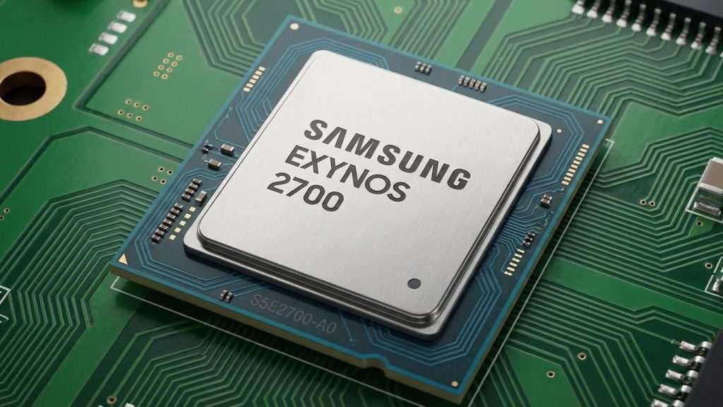
The Taylor facility, known as Plant 1, will act as the testing ground for the installation, etching, and deposition processes essential for EUV technology. Full-scale production is anticipated to begin in the latter half of 2026. While specifics about manufacturing Samsung’s own Exynos 2600 chips at this site remain unconfirmed, the plant is slated to produce Tesla’s autonomous driving chips, AI5 and AI6, under a substantial $16.5 billion partnership between the two companies.
Scale and Workforce: Preparing for Mass Production
To ensure the Taylor plant meets all operational standards, Samsung plans to apply for a Temporary Certificate of Occupancy (TCO) from local authorities, confirming compliance with fire safety and other regulations. The company has deployed an impressive workforce of 7,000 employees on-site to expedite construction and setup. Once complete, the six-storey building will accommodate around 1,000 staff members. The sheer scale of the facility is notable, spanning approximately 4.85 million square metres, surpassing Samsung’s other major foundries in Pyeongtaek and Hwaseong.
Samsung’s foresight in securing ample land at the Taylor site allows for expansion, with plans to establish up to 10 plants in the future. This strategic move positions Samsung to scale its production capacity significantly as demand for advanced semiconductors grows.
The Importance of EUV Technology and Financial Challenges
Acquiring EUV machines from ASML is a costly but essential step for Samsung to achieve high-yield production of 2nm GAA wafers. Current yield rates on Samsung’s cutting-edge lithography are estimated at around 50 percent, highlighting the need for sophisticated equipment to improve efficiency and profitability. Each EUV machine costs roughly 500 billion won (approximately $339.3 million), representing a substantial investment amid Samsung’s reported deficit of $680 million projected for the third and fourth quarters of 2025.
Despite these financial challenges, Samsung aims to turn its foundry business profitable by 2027. The company’s commitment to deploying advanced EUV technology and expanding its manufacturing footprint in the US reflects a strategic effort to compete with rivals and meet growing global semiconductor demand.
Context and Future Outlook
Previously, the Taylor plant was intended for 4nm chip production. However, with TSMC opting not to bring its most advanced technologies to the US, Samsung has seized the opportunity to fill this gap. The initial mass production target for the facility is set at 50,000 wafers, signalling a significant scale for a new manufacturing site.
As Samsung continues to develop its US-based semiconductor capabilities, the industry will be watching closely to see how the Taylor plant’s operations evolve. The successful ramp-up of 2nm GAA wafer production could mark a pivotal moment for Samsung and the broader semiconductor landscape.
For further details on Samsung’s semiconductor ambitions and EUV technology deployment, see the insightful report from the Korea Economic Daily.
Looking ahead, Samsung’s progress with the Taylor plant will be a key indicator of its ability to compete in the advanced chip manufacturing arena, especially as it aims for profitability and expanded production capacity in the coming years.