Samsung Achieves Significant Milestone in 2nm GAA Technology
Samsung has reportedly reached a 50 percent yield rate on its 2nm Gate-All-Around (GAA) semiconductor manufacturing process, marking a notable advancement in its next-generation chip production capabilities. This development comes as the South Korean tech giant prepares to promote its second-generation 2nm GAA node, known as SF2P, to foundry customers. The move indicates Samsung’s commitment to refining its cutting-edge manufacturing technology and expanding its client base.
Details on SF2P and Future Plans
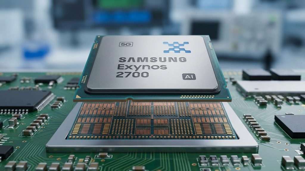
The SF2P node, which represents the second iteration of Samsung’s 2nm GAA technology, offers several improvements over the initial generation. Samsung has already completed the basic design of this process, with the design solution partners receiving guidelines to actively promote SF2P rather than the earlier SF2. This shift suggests that Samsung is prioritising resources towards the newer manufacturing process, which is expected to underpin next year’s Exynos 2700 chipset. The upcoming SoC is rumoured to support advanced features such as LPDDR6 RAM and UFS 5.0 storage, signalling a significant performance boost.
Besides Samsung’s own chipsets, the SF2P node is also set to be used for Tesla’s AI6 chips, following a substantial $16.5 billion agreement between the two companies. Furthermore, Chinese cryptocurrency mining equipment manufacturers MicroBT and Canaan have reportedly placed orders for 2nm GAA chips with Samsung, underlining the growing confidence in Samsung’s manufacturing capabilities within diverse industries.
Context and Challenges Ahead
When Samsung began mass production of its Exynos 2600 in September 2025, the 2nm GAA yields were estimated at 50 percent, with a target of reaching 70 percent. While there has been no further yield improvement since then, this 50 percent rate is a considerable leap compared to Samsung’s 3nm GAA technology, which struggled to surpass a 30 percent yield and consequently faced difficulties in attracting customers. The company anticipates only incremental yield improvements for the first-generation 2nm process as it shifts focus to SF2P.
Looking further ahead, Samsung is already working on its third-generation 2nm GAA process, dubbed SF2P+, which is expected to be ready within two years. Despite these advancements, Samsung still faces a challenging road to rival semiconductor leader TSMC, but it aims to achieve profitability in its foundry business by 2027, laying the groundwork for future competitiveness.
What to Expect Next
Samsung’s progress with its 2nm GAA technology and the promotion of the SF2P node highlight its strategic push to enhance semiconductor manufacturing and attract high-profile customers. As the company prepares to integrate this technology into flagship chipsets and expand partnerships, the industry will be watching closely to see how Samsung’s yields improve and how quickly it can scale production. The coming years will be crucial as Samsung strives to establish itself as a formidable player in advanced semiconductor fabrication.
Source: ZDNet