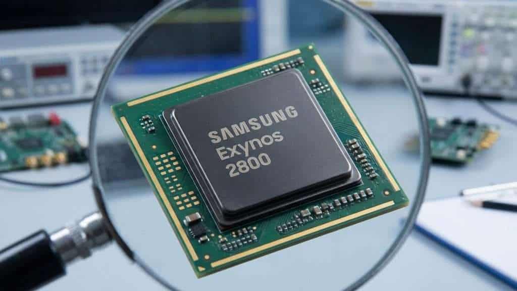
Samsung Develops New ‘Side By Side’ Packaging for Exynos Chips
Samsung is advancing its Exynos chipset technology with a new packaging method known as ‘side by side’ (SbS), designed to improve heat dissipation and reduce the overall thickness of the chipset package. This new structure positions the chipset die and DRAM horizontally adjacent to each other, with a Heat Pass Block (HPB) placed on top of both components. This configuration allows heat to dissipate more rapidly, potentially leading to better thermal management and improved performance.
Key Features and Benefits of the Side By Side Packaging
The SbS packaging differs from previous methods Samsung has employed, such as the Fan-out Wafer Level Packaging (FOWLP) used in the Exynos 2400 and the Heat Pass Block technology introduced with the Exynos 2600, Samsung’s first 2nm GAA SoC. By placing the dies side by side, Samsung can reduce the thickness of the chipset package, which could be particularly advantageous for future smartphones aiming for a slimmer profile. This innovation might even pave the way for a return of the Galaxy S26 Edge or similar devices that benefit from a thinner design.
Moreover, smartphone manufacturers interested in producing thinner devices could leverage this packaging technology, provided they adopt Samsung’s 2nm GAA process. While the Exynos 2600 is reportedly being tested for the Galaxy Z Flip 8, it is unlikely that the SbS packaging will debut on that foldable model. However, Samsung’s strategy might evolve to incorporate this packaging in devices where compactness and heat management are critical.
Context and Future Prospects for Exynos Chipsets
Although there is no official confirmation regarding the Exynos 2700 incorporating the SbS packaging, it is considered a strong candidate for this technology. The upcoming Exynos 2800, expected to feature a GPU designed entirely in-house by Samsung, is also likely to adopt the new packaging. Given that this next-generation chipset is anticipated to be used across various device categories beyond smartphones, the benefits of the SbS structure could be even more pronounced.
Samsung has consistently pushed the boundaries of semiconductor packaging to enhance performance and efficiency. The progression from FOWLP to HPB and now to SbS packaging reflects the company’s commitment to innovation in its Exynos lineup. These advancements not only improve thermal performance but also support the trend towards thinner, more powerful mobile devices.
What to Expect Next
As Samsung continues to develop and refine the ‘side by side’ packaging, we can expect future Exynos chipsets to offer improved thermal management and potentially enable slimmer smartphone designs. Industry watchers will be keen to see which upcoming devices first feature this technology and how it impacts overall device performance and form factor. With Samsung’s 2nm GAA process at the core, the SbS packaging represents a promising step forward in mobile chipset engineering.
For more details on Samsung’s chipset innovations, see the recent report from ZDNet.