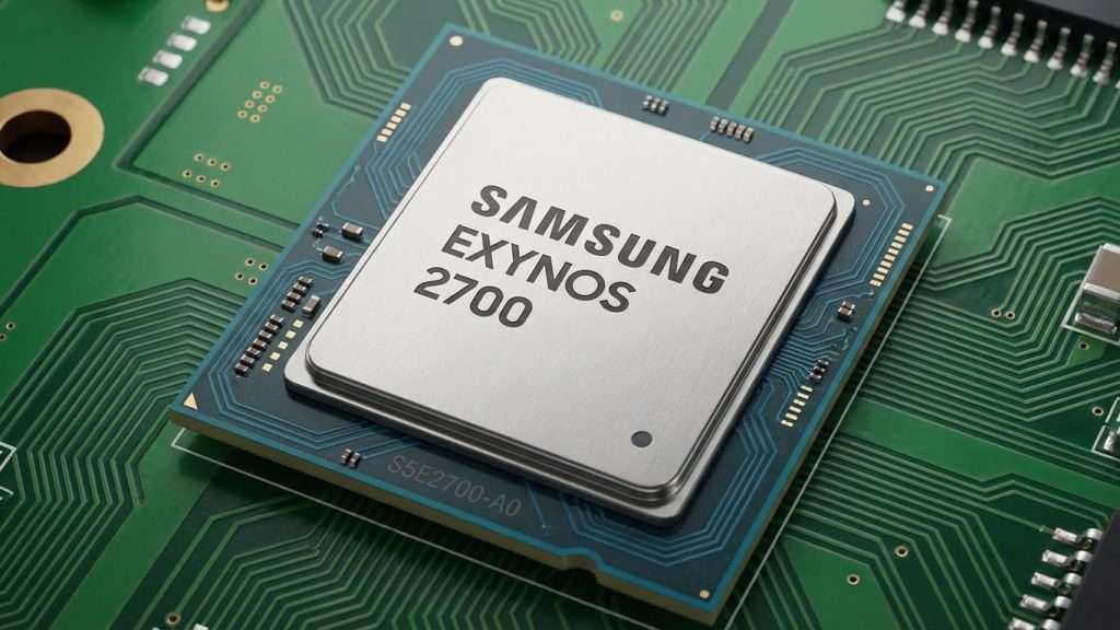
Exynos 2700 Leak Reveals Impressive Technical Upgrades
Samsung’s upcoming Exynos 2700 chip, internally codenamed Ulysses, is shaping up to be a significant leap forward in mobile SoC technology. Expected to launch in 2027, this new processor aims to address the thermal limitations seen in its predecessor, the Exynos 2600, while delivering substantial performance and efficiency improvements. A recent leak from a relatively obscure tipster, whose credibility is bolstered by recognition from a prominent Samsung leaker on X, has shed light on the chip’s key specifications and architectural innovations.
Key Features and Specifications
The Exynos 2700 will be manufactured using Samsung’s advanced SF2P process, a next-generation iteration of the 2nm Gate-All-Around (GAA) technology introduced with the Exynos 2600. This new process promises a 12% increase in overall performance and a 25% reduction in energy consumption compared to the previous SF2 node. Notably, the prime core’s clock speed is expected to rise to 4.20GHz, up from 3.90GHz in the Exynos 2600, potentially boosting single-core performance significantly.
In terms of CPU architecture, the Exynos 2700 is anticipated to utilise ARM’s latest C2 cores, which have replaced the older Cortex naming scheme. While the exact core configuration remains unconfirmed, it is likely Samsung will maintain a similar 1+3+6 setup as seen in the Exynos 2600. The new cores are expected to deliver around a 35% increase in instructions per cycle (IPC), translating to theoretical Geekbench 6 scores of approximately 4,800 for single-core and 15,000 for multi-core tests. This represents a 40% and 30% improvement respectively over the current generation.
Another major upgrade involves the chip’s packaging technology. The Exynos 2700 will reportedly adopt FOWLP-SbS (Fan-Out Wafer-Level Packaging – Side-by-Side) with a unified Heat Path Block. This copper-based heat sink covers the entire application processor and DRAM, enabling more efficient heat dissipation than the partial coverage seen in the Exynos 2600. This design shift should help mitigate thermal bottlenecks, a common challenge in high-performance mobile chips.
GPU and Memory Enhancements
Samsung is expected to continue integrating AMD architecture-based Xclipse GPUs in the Exynos 2700, which will benefit from faster data transmission speeds thanks to support for LPDDR6 RAM and UFS 5.0 storage standards. LPDDR6 offers throughput up to 14.4 Gbps, while UFS 5.0 further accelerates data access. These improvements could yield a 30-40% performance boost in graphics and overall system responsiveness. It is worth noting that some recent rumours suggest Samsung might shift to an in-house GPU design with the subsequent Exynos 2800 chip, but the 2700 will likely retain the AMD-based GPU.
Context and What to Expect Next
The Exynos 2700’s development reflects Samsung’s ongoing efforts to enhance its in-house chipsets and reduce reliance on Qualcomm’s Snapdragon processors, which currently dominate many flagship devices. The improvements in thermal management, processing power, and memory technology position the 2700 as a strong competitor against upcoming Snapdragon chips like the Snapdragon 8 Elite Gen 5. However, some details remain unclear, such as whether the Exynos 2700 will feature an integrated modem, which could impact efficiency and manufacturing complexity.

As Samsung prepares for a 2027 launch, enthusiasts and industry watchers will be keen to see official announcements and further details. The Exynos 2700’s advancements in process technology, core architecture, and packaging could mark a pivotal moment for Samsung’s semiconductor ambitions, potentially reshaping the competitive landscape of premium smartphone chips.
Overall, the Exynos 2700 leak offers an exciting glimpse into Samsung’s future plans, signalling notable progress in performance and thermal efficiency that could benefit next-generation Galaxy devices and beyond.
Source: Twitter